
How Ozone Is Used in Semiconductor Cleaning Processes
How Ozone Is Used in Semiconductor Cleaning Processes
Semiconductor manufacturing demands cleanliness standards that are difficult to imagine. A single speck of dust or trace organic residue on a silicon wafer can destroy an entire batch of chips. As device geometries shrink and wafer complexity increases, traditional chemical cleaning methods are being replaced or supplemented by processes that are faster, greener, and more precise. Ozone has emerged as one of the most powerful tools in this evolution.
This article explains how ozone is used in semiconductor cleaning processes, why it outperforms many legacy chemistries, and how fabs monitor ozone concentration to protect both product quality and worker safety.
Why Semiconductor Cleaning Demands Extreme Purity
Modern integrated circuits are built through hundreds of sequential process steps. At each stage, wafers are exposed to photoresists, etchants, metals, and airborne particles. Any contaminant left on the surface can cause:
- Defective patterns during lithography
- Poor adhesion of thin films in deposition steps
- Unintended electrical characteristics in transistors and interconnects
- Yield loss that translates directly into higher production costs
Because of these risks, wafer cleaning is not a single step but a recurring discipline woven throughout the production flow. Cleaning steps can account for more than 30% of all manufacturing operations in a leading-edge fab. The goal is to leave surfaces atomically clean without damaging delicate structures or introducing new contaminants.
How Ozone Cleans at the Molecular Level
Ozone (O₃) is one of the strongest oxidizing agents available for industrial use. When ozone contacts organic molecules such as oils, photoresist residues, or airborne hydrocarbons, it breaks carbon-carbon and carbon-hydrogen bonds through oxidation. The reaction converts these contaminants into carbon dioxide, water, and other volatile or soluble species that can be rinsed away.
In semiconductor cleaning, ozone is typically delivered in two forms:
- Gas-phase ozone: Used for dry stripping of photoresist and surface modification in controlled chambers.
- Ozonated deionized water (DI-O₃): Used for wet cleaning, final rinsing, and particle removal in baths or single-wafer tools.
Unlike aggressive acids such as sulfuric peroxide mixtures, ozone can be generated on-site from pure oxygen or dry air and leaves no chemical residue when it decomposes back to oxygen. This makes it attractive for fabs seeking to reduce chemical consumption, lower disposal costs, and improve environmental performance.
Key Semiconductor Cleaning Applications for Ozone
Wafer Surface Preparation
Before critical steps such as gate oxidation, epitaxial growth, or atomic layer deposition, wafers must be free of organic and metallic contamination. Ozonated water effectively removes organic films and particles while adding minimal metallic contamination compared to traditional RCA cleans. In many fabs, ozone-based cleans have replaced or reduced the use of sulfuric acid-hydrogen peroxide mixtures (SPM) and ammonium hydroxide-hydrogen peroxide mixtures (SC-1).
Photoresist Stripping
Photoresist is essential for patterning wafers, but it must be completely removed after etch or ion implantation. Ozone-based dry stripping offers an attractive alternative to plasma ashing because it generates less plasma-induced damage and fewer particle defects. In single-wafer spray tools, a combination of ozone gas and heated deionized water can strip advanced resists without attacking sensitive low-k dielectric films.
Organic Contamination Removal
Trace organic contamination from packaging materials, cleanroom air, or handling equipment can migrate onto wafer surfaces. Ozone reacts selectively with these contaminants, breaking them into small molecules that dissolve in water or evaporate as gas. For high-purity cleaning loops, ozone concentration must be maintained within a tight window: too little leaves residue, while too much can roughen silicon surfaces or oxidize metal films.
Monitoring Ozone in Cleaning Processes
Effective ozone cleaning depends on precise control of ozone concentration, flow rate, exposure time, and temperature. This is where gas-phase ozone monitors and dissolved ozone analyzers become indispensable.
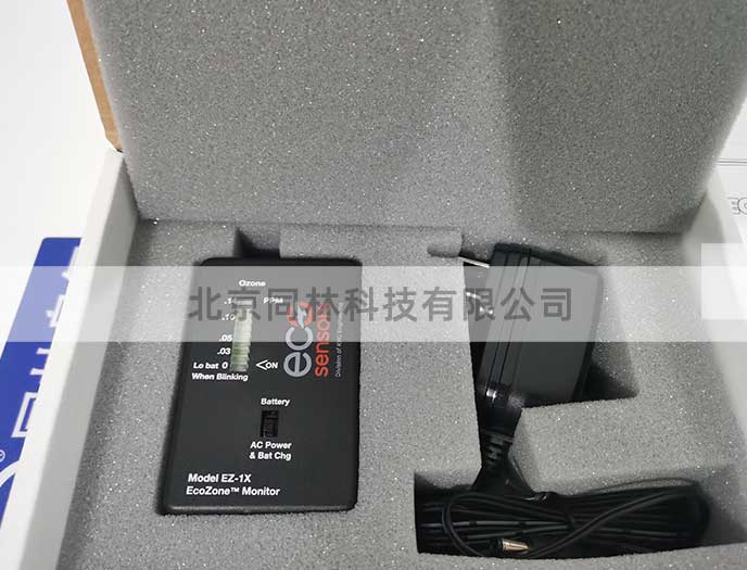
UV absorption ozone analyzers are particularly well suited for semiconductor environments. They measure ozone concentration by detecting the absorption of UV light at 254 nm, providing real-time readings without consuming reagents. For wet cleaning tools, dissolved ozone monitors track the concentration of ozone in deionized water and provide feedback to ozone generators and dosing systems.
Key monitoring requirements include:
- Sub-ppb to ppm range to cover both trace leakage detection and process concentration control
- Fast response time for closed-loop control in dynamic single-wafer processes
- Low drift and long calibration intervals to minimize tool downtime
- Cleanroom-compatible materials such as stainless steel and fluoropolymers
- Digital interfaces such as RS-485, Modbus, or Ethernet for integration with fab SCADA systems
If you need help selecting the right analyzer for your cleaning process, request a quotation and our applications team will recommend a configuration matched to your requirements.
Safety and Environmental Considerations
While ozone is a valuable cleaning agent, it is also toxic at elevated concentrations. Occupational exposure limits vary by region, but most authorities set ceiling levels around 0.1 ppm for an 8-hour time-weighted average. Fabs must install ambient ozone monitors near process tools, exhaust lines, and personnel access points to detect leaks before they become hazardous.
For detailed guidance on permissible exposure limits and workplace controls, refer to the OSHA guidelines on occupational exposure limits. Proper ventilation, interlocked alarms, and continuous ozone monitoring are essential elements of a safe semiconductor cleaning operation.
From an environmental perspective, ozone-based cleaning reduces the volume of hazardous chemical waste generated by traditional wet benches. Because ozone reverts to oxygen, facilities can often simplify their waste treatment infrastructure while improving cleaning performance.
Conclusion
Ozone has become a cornerstone of modern semiconductor cleaning, offering powerful oxidation, residue-free decomposition, and compatibility with increasingly delicate device structures. Whether used in gas-phase dry stripping or ozonated water wet cleans, ozone helps fabs achieve the extreme cleanliness required for advanced node production.
Successful implementation depends on precise ozone measurement and control. Beijing Linji Environmental Technology Co., Ltd. supplies gas ozone monitors and dissolved ozone analyzers engineered for demanding semiconductor applications. Contact us to discuss your process requirements and find the right monitoring solution for your fab.
 Case Study: Ozone Monitoring i
 Ozone Monitoring in Food &
 The History of Ozone Detection
How Ozone Is Used in Semicondu
The History of Ozone Detection
How Ozone Is Used in Semicondu